Table of Contents >> Show >> Hide
- Why SMD prototyping gets messy so fast
- What Stamp is (and why it’s different)
- Where Stamp fits in the prototyping spectrum
- How to prototype with Stamp: a practical workflow
- Concrete example: an ATtiny85 breakout module
- Assembly tips: make SMD soldering feel less like a boss fight
- Prototyping patterns that work especially well with Stamp
- Is Stamp right for your bench?
- Field Notes: of Real-World “Stamp Life”
- Conclusion
Surface-mount devices (SMDs) are the default language of modern electronics. They’re tiny, fast, inexpensive, andif we’re being honestkind of smug about it. Meanwhile, the classic solderless breadboard is still living its best 1970s life, waiting for a 0.1″ DIP package that may never return from war.
That mismatch is exactly where Stamp modular breakout boards come in: a system designed to make SMD prototyping feel more like snapping together neat little “circuit blocks,” and less like wrestling a plate of spaghetti made of jumper wires and regret.
Why SMD prototyping gets messy so fast
If you’ve ever tried to prototype a circuit with an SOT-23 regulator, a QFN sensor, and a few 0603 passives on a breadboard, you already know how the story ends: you either (1) give up and order a PCB, (2) buy a random breakout board that’s “close enough,” or (3) build a precarious adapter tower that collapses the moment you look at it.
Breadboards weren’t built for tiny packages
Breadboards excel at through-hole parts and dual-inline packages. But with SMD parts, you’re forced into adapters and flying leads. That adds three classic problems:
- Mechanical fragility: a small bump becomes a “why did the UART stop working?” mystery.
- Troubleshooting pain: probing a circuit shouldn’t feel like defusing a bomb.
- Iteration slowdown: each revision becomes either a rewire marathon or a new PCB order.
Typical breakout boards help… but don’t always scale
Standard breakout boards are great for bringing a single IC to headers. But real circuits usually need more than “the chip, and vibes.” You want decoupling capacitors close to power pins, pull-ups where they belong, indicator LEDs sometimes, and a clean way to route power and ground. That’s where many one-off breakouts start to feel like unfinished sentences.
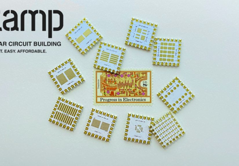
What Stamp is (and why it’s different)
Stamp is a modular family of template breakout PCBs designed specifically for building small SMD “modules” that connect together. Think: breakout boards, but with a system-level mindsetpower distribution, compact footprints, and module-to-module interconnect built in.
A tiny PCB “tile” that can hold a real sub-circuit
Each Stamp is designed around a particular footprint (for example, a specific SOIC pattern). The practical idea is simple: put the main IC on the front, and place supporting passives on the back. Instead of spreading components across a breadboard (and across your entire emotional range), you keep the circuit tight and reproducible.
One example build uses a SOIC-10 Stamp layout matched to an ATtiny85 in a SOIC-8 package, while leaving room for 0603 parts and indicator LEDs. That’s the kind of “not just a breakout, but a usable mini-board” approach Stamp is aiming for.
Modular interconnects that don’t require a jumper-wire sacrifice
The Stamp concept leans heavily into edge connectionsso you can link boards side-by-side (and in some cases at right angles). The result is a modular, reconfigurable prototype that looks more like a tidy assembly than a breadboard crime scene.
Power routing that’s designed innot duct-taped on
A detail that matters in practice: Stamp boards can include dedicated power routing pads that let you bridge VCC and GND across the module. In the ATtiny85 example, simple solder bridges connect power between sides of the Stamp and tie certain pins to rails cleanlywithout adding long external jumpers.
Where Stamp fits in the prototyping spectrum
Stamp is best understood as a “middle layer” between: (A) breadboards (fast but messy for SMD) and (B) custom PCBs (clean but slower and less forgiving for iteration).
Compared to classic breakout boards (Adafruit/SparkFun-style)
Traditional breakout boards shine when you want to test a specific chip quickly and don’t mind the rest of the circuit being external. Stamp’s pitch is different: build the chip plus its supporting cast on the same small board, then connect modules like building blocks. It’s a workflow upgrade when your prototype keeps growing beyond “one sensor on one breakout.”
Compared to SMD prototyping helpers like Schmartboard
Products that make hand-soldering fine-pitch parts easier are awesomeespecially when you’re adapting a tricky package to something breadboard-friendly. Stamp’s differentiator is its modular “tile” approach: you’re not just escaping fine pitch; you’re building a set of compact functional modules that connect in a repeatable way.
Compared to Manhattan / dead-bug prototyping
Manhattan prototyping on copper-clad can be wonderfully fast, and it’s popular for analog and RF work because you can keep leads short and use the copper as a ground plane. Stamp targets a different use case: structured, reusable modules for common SMD footprintsmore “mini PCBs” than “artisan electronics sculpture.”
Compared to ordering quick-turn custom PCBs
Custom PCBs are still the endgame for anything you’ll ship or repeat. But for early explorationchoosing a regulator, validating a sensor chain, iterating on a buck converterStamp aims to reduce the “spin a board, wait, revise, repeat” loop.
How to prototype with Stamp: a practical workflow
1) Decide what your “modules” are
Prototypes get cleaner when you treat them like systems. Instead of “one big blob circuit,” break your design into blocks: power, compute, sensing, level shifting, connectors. Stamp is designed to support exactly that kind of modular decomposition.
2) Build each module as a compact, testable unit
The secret to fast iteration is testable boundaries. For each Stamp module:
- Place the main IC on the front (the footprint defines the “core”).
- Add required passives on the back (decoupling, pull-ups, feedback networks, indicator LEDs).
- Use built-in routing pads where available to join VCC/GND rails and simplify wiring.
- Add labeled I/O connections so your future self doesn’t need therapy.
3) Connect modules in a layout that matches your debugging style
Some people debug like surgeons (precise, calm). Others debug like raccoons (fast, chaotic, snacks). Stamp leans toward the surgeon method: keep modules neatly connected, with clear access points for probes and rework.
Concrete example: an ATtiny85 breakout module
A published build example uses a SOIC-10 Stamp matched to an ATtiny85 in SOIC-8, with the front side optimized for 0603 components. The idea is to build a complete, usable microcontroller “tile”:
- Front: the ATtiny85 plus a GPIO indicator LED.
- Back: resistors/capacitors and a power indicator LED.
- Power routing: solder-bridge pads that connect VCC across the Stamp and connect GND across the Stamp, plus bridges tying pins to rails where needed.
This is where Stamp feels different from a basic breakout: you’re not just converting pin pitchyou’re building a compact sub-circuit with the “boring but critical” parts (like decoupling and indicators) already living where they should.
Assembly tips: make SMD soldering feel less like a boss fight
You don’t need a factory line to build SMD modules, but you do need a plan. Here are practical tips that pair well with Stamp breakout boards and other SMD prototyping boards.
Use the right technique for the package
- SOIC/TSSOP: flux + drag soldering works great. Clean up bridges with wick, then pretend it was intentional.
- 0603/0805 passives: tweezers + a small solder bead is fast; solder paste + hot air is even faster once you’re comfortable.
- QFN/LFCSP (thermal pad): consider solder paste and hot air/reflow so the exposed pad actually bonds. If the belly pad doesn’t solder, the part may “work” until it doesn’t.
Hot air and solder paste: the “fast prototyping” combo
For many Stamp-style builds, solder paste plus hot air reflow is the sweet spot: you can place multiple parts quickly and reflow them with less risk of lifting pads. Start with low airflow, keep the nozzle moving, and let the solder’s surface tension do the alignment work.
Common SMD pitfalls (and how to avoid them)
- Tombstoning: heat both pads evenly; don’t flood one side with paste.
- Bridging on fine pitch: use more flux than you think you need; then add a little more.
- Overheating: preheat gently, then reflow; don’t park hot air like it’s a camping chair.
- Moisture sensitivity: some packages are sensitive to moisture/reflow stressstore parts properly and follow handling guidance when applicable.
Prototyping patterns that work especially well with Stamp
Create a “power spine” first
Build a dedicated power module (regulator + filtering + protection), validate it, then reuse it while iterating other blocks. In modular prototyping, power problems are the #1 way to waste an afternoon and #2 way to invent new words.
Put test access on the edges
Whether you’re using edge soldering or headers, prioritize having: VCC, GND, and the key signals easy to probe. A clean modular system is only as good as your ability to measure it.
Design your modules around “swap points”
If you’re evaluating two regulators or two sensors, make the rest of the system stable and swap only the target module. Stamp’s modularity is most valuable when it reduces variables during debugging.
Is Stamp right for your bench?
Stamp makes the most sense if you:
- Prototype with SMD parts often and want a cleaner workflow than breadboards + adapters.
- Iterate frequently and hate waiting on PCB revisions for every small change.
- Prefer reusable building blocks (power, compute, sensing) over one-off “temporary” wiring that becomes permanent by accident.
You might choose a different approach if you:
- Work primarily with through-hole parts and only occasionally touch SMD.
- Need very specialized footprints or unusual mechanical constraints right away (custom PCBs may be faster).
- Are prototyping high-frequency or ultra-low-noise analog circuits where layout and grounding strategy are the whole game (Manhattan/copper-clad can be excellent).
Field Notes: of Real-World “Stamp Life”
The first time you build a modular SMD prototype, you’ll probably do what I did: assemble a “simple” power module, plug it into a microcontroller module, add a sensor module, and immediately assume you’ve invented a new, cleaner universe. Then the LED doesn’t light, and you remember the universe still includes you.
My favorite part of the Stamp concept is how it nudges you into good habits. On a breadboard, it’s easy to treat decoupling capacitors like optional side quests. On a compact Stamp module, they’re right therephysically close, logically obvious, and far less likely to be “added later” (translation: never). That alone can turn a flaky prototype into something that behaves like a real circuit.
The second big win is iteration speed. I built a small controller block, then decided I wanted a different reset behavior. On a breadboard, that would have meant re-routing wires and hoping the connection quality stayed consistent. In a modular system, I could treat the change like a module edit: update the pull-up, swap a component value, reflow, retest. The mental model is cleaner: you’re editing a known sub-circuit, not re-laying an entire nest.
Of course, compactness has its own “gotchas.” The first time I used solder paste, I applied it like frostingbecause I am an optimist and also a fool. Result: bridges, messy joints, and a brief moment where I considered taking up woodworking. The fix was surprisingly simple: less paste, more flux, and a slower, more even heat ramp. Once I dialed that in, hot air reflow became the fastest way to populate a moduleespecially when multiple 0603 parts were involved.
Another lesson: pick a consistent power strategy and stick to it. When you’re connecting modules, a single “oops, that rail is actually 3.3 V” moment can ruin your day. I started labeling modules with a paint marker (VCC: 5V / 3V3, GND, I2C/SPI/UART), and suddenly everything got calmer. Also: build a known-good “power spine” first. Having stable rails makes debugging everything else dramatically easier.
The most satisfying moment, though, was when the prototype stopped looking like a prototype. Modular boards connected cleanly, signals were easy to probe, and changes didn’t destroy the whole setup. That’s the quiet superpower of a system like Stamp: it doesn’t just make SMD possibleit makes iteration feel organized. And if your bench has ever looked like a jumper-wire explosion, you’ll understand why that’s worth celebrating.
Conclusion
Stamp modular breakout boards aim to modernize the “quick prototype” experience for SMD parts: compact modules, built-in routing patterns, and interconnects designed for iteration. If you’re tired of breadboard chaos but not ready to spin a PCB for every idea, Stamp is the kind of middle-ground tool that can make prototyping faster, cleaner, and (most importantly) easier to debug.